Structure and working principle
Since the transmission electron microscope is imaged by TE, this requires that the thickness of the sample must be within the size range that the electron beam can penetrate. To this end, it is necessary to transform large-sized samples to an acceptable level for transmission electron microscopy through various cumbersome sample preparation methods.
Whether it can directly use the material properties of the sample surface material for microscopic imaging has become the goal pursued by scientists.
After hard work, this idea has become a reality ----- scanning electron microscope (ScanningElectronicMicroscopy, SEM).
SEM is an electronic optical instrument that uses a very fine electron beam to scan the surface of the sample to be observed, and collects a series of electronic information generated by the interaction between the electron beam and the sample, which is transformed and amplified to form an image. It is a useful tool for studying three-dimensional surface structure.
Its working principle is:
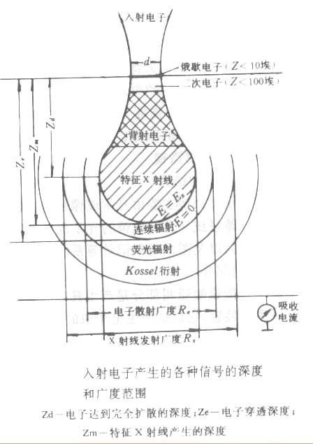
In the high-vacuum lens barrel, the electron beam generated by the electron gun is focused into a thin beam by the electron converging lens, and is scanned and bombarded point by point on the sample surface to generate a series of electronic information (secondary electrons, back-reflected electrons, transmitted electrons, absorption Electronics, etc.), various electronic signals are received by the Detector, amplified by the electronic amplifier, and then input to the picture tube controlled by the picture tube grid.
When the focused electron beam scans the surface of the sample, due to the different physical and chemical properties, surface potential, elemental composition and concave-convex shape of the surface of different parts of the sample, the electronic information excited by the electron beam is different, resulting in the electron beam of the picture tube The intensity also changes continuously, and finally an image corresponding to the surface structure of the sample can be obtained on the fluorescent screen of the kinescope. Depending on the electronic signal received by the Detector, the backscattered electron image, secondary electron image, absorption electron image, etc. of the sample can be obtained respectively.
The resolution of the scanning electron microscope can reach 50~100Å, and the electron magnification can be continuously changed from a dozen times to hundreds of thousands of times. The entire surface of the sample can thus be observed more closely.


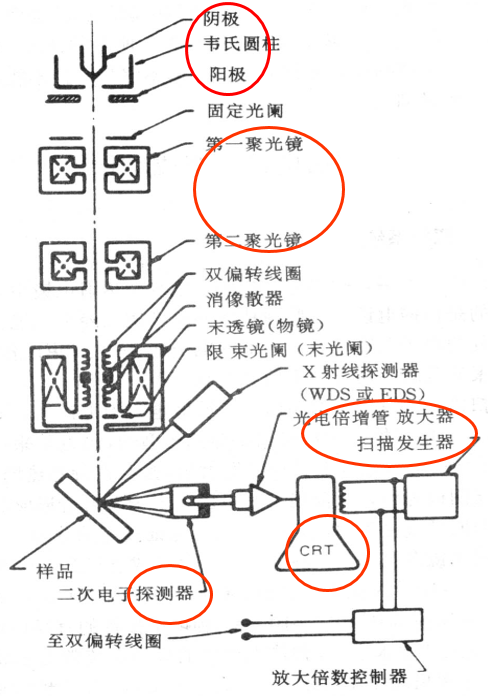
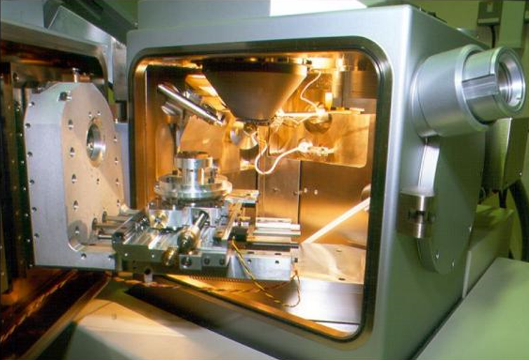
1. Electron optical system
<1> Electron gun: The function is to use the high voltage between the cathode and the anode filament to generate a high-energy electron beam. Most current SEMs use hot cathode electron guns.
<2> Electromagnetic lens: The main function is to gradually reduce the beam spot of the electron gun, which is to shrink the original beam spot with a diameter of about 5um into a small beam spot with only a few um.
<3>Scanning coil: The function is to provide the synchronous scanning signal of the incident electron beam on the surface of the sample and on the fluorescent screen.
<4>Sample chamber: The sample stage can move, tilt and rotate in three-dimensional space, and various types of Detectors can be installed.
2. Signal detection and amplification system
作用是检测样品在入射电子作用下产生的物理信号,然后经视频放大作为显像系统的调制信号。
3、真空系统和电源系统
作用是为保证电子光学系统正常工作,防止样品污染提供高的真空度。电源系统由稳压,稳流及相应的安全保护电路所组成,其作用是提供扫描电镜各部分所需稳定电源。
1、放大倍数
由于扫描电镜的荧光屏尺寸是固定不变的,因此,放大倍率的变化是通过改变电子束在试样表面的扫描幅度来实现的。
如果减少扫描线圈的电流,电子束在试样上的扫描幅度将减小,放大倍数将增大。调整十分方便,可从20倍连续调节到20万倍左右。
2、分辨率
分辨率是扫描电镜的主要性能指标。
分辨率大小由入射电子束直径和调制信号类型共同决定:
电子束直径越小,分辨率越高。
用于成像的物理信号不同,分辨率不同。
例如SE和BE电子,在样品表面的发射范围也不同,其分辨率不同。一般SE的分辨率约为5-10nm,BE的分辨率约为50-200nm。
3、景深
是指一个透镜对高低不平的试样各部位能同时聚焦成像的一个能力范围。
扫描电镜的末级透镜采用小孔径角,长焦距,所以可以获得很大的景深,它比一般光学显微镜景深大100-500倍,比透射电镜的景深大10倍。
景深大,立体感强,形态逼真是SEM的突出特点。
用于扫描电镜的试样分为两类:
一是导电性良好的试样,一般可以保持原始形状,不经或稍经清洗,就可放到电镜中观察;
二是不导电的试样,或在真空中有失水、放气、收缩变形现象的试样,需经适当处理,才能进行观察。
对于导电性不好或不导电的试样,如高分子材料、陶瓷、生物试样等,在入射电子照射下,表面易积累电荷,严重影响图像质量。
因此对不导电的试样,需要进行真空镀膜,在试样表面蒸镀一层厚约10nm的金属膜或碳膜,以避免荷电现象。
采用真空镀膜技术,除了能防止不导电试样产生荷电外,还可增加试样表面的二次电子发射率,提高图像衬度,并能减少入射电子束对试样的辐射损伤。
The sample can be block or powder particles, which can keep stable in vacuum, and the sample containing moisture should be dried to remove the moisture first. The sample whose surface is polluted should be properly cleaned without destroying the surface structure of the sample, and then dried;
Newly broken fractures or sections generally do not need to be treated, so as not to damage the structural state of the fracture or surface.
The surface and fracture of some samples need to be properly eroded to expose some structural details, so the surface or fracture should be cleaned after erosion, and then dried. The magnetic sample should be demagnetized in advance to prevent the electron beam from being affected by the magnetic field during observation.
The size of the sample should be suitable for the size of the special sample holder of the instrument, and it should not be too large. When placing samples of different sizes, the height of the samples is also limited, generally around 5-10mm.

