The electrical, optical, and other properties of thin films often differ from those of bulk materials. The conditions present on the substrate during deposition have a strong influence on these properties. When the sputtered atoms condense on the substrate, it converts kinetic energy into the surface lattice. The resulting loosely bound atoms are mobile at the surface and migrate across the surface, interacting with other adatoms until they find a persistent low energy point, or are desorbed. As the film thickness increases, the atoms in the lattice move to more stable positions through bulk diffusion.
For many metals, the mobility of surface and bulk atoms is related to the substrate temperature (T) and the metal melting point (TM). At low T/Tm values, surface and bulk diffusion play only a small role because the atoms do not have enough energy to move from their initial positions. Films deposited under these conditions (Fig. 31.8) have an unclear internal crystal structure and many defects; voids are also present due to shadowing effects. Conditions that tend to produce lower T/TM are higher melting point target materials (e.g., refractory metals), heat sinking substrates, higher operating pressures (i.e. "thermalization" or reduced energy of the sputtered atoms), and Reactive gases adsorb on the surface. A higher T/T m value leads to surface diffusion and volume diffusion of the grown film, resulting in dense columnar grains with fewer defects and clear boundaries.
In addition to substrate heating, T can be effectively increased by bombarding the substrate with ions or electrons during deposition. In diode systems, the substrate is usually in a plasma, which heats up the film due to energetic electron collisions. A bias voltage can also be applied to the substrate to accelerate incoming ions, increasing the kinetic energy transferred to the surface. When depositing alloys or compounds, a higher T value may lower the adhesion coefficient of one component, thereby charging the entire film composition. One thing to note is that the kinetic energy of the sputtered atoms is typically 10 times that of the evaporated species. This factor plays an important role in determining the difference between sputtered and evaporated thin films.
Most sputtered films are under compressive or tensile stress. The stress is due to the thermal expansion coefficient mismatch between the substrate and the film, as well as the internal stress of the film due to lattice defects. In high TM materials, deposited at low T/T m, internal stresses usually dominate and may reach the film yield strength, leading to fracture. Working air pressure has an effect on the magnitude and type of internal stresses. Thermal stress dominates in high T/TM coatings.
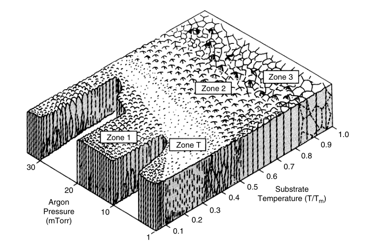
Figure 1. Schematic representation of the relationship of substrate temperature and argon pressure to the structure of a metal coating sputtered with a cylindrical magnetron. t is the substrate temperature and t is the melting point of the coating material. (JA Thornton, In Thin Film Deposition Technology, R.F. Bunshah, ed. Ridge Park, NJ: Noyce Publications, 1982, p. 214.)