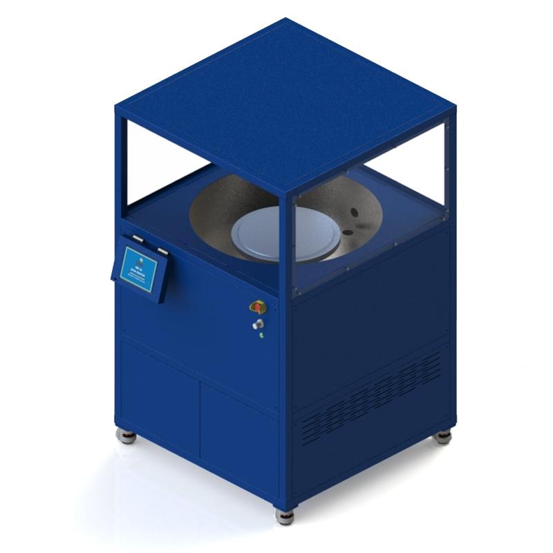
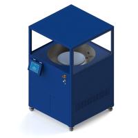
Spin coating is a widely used method for uniformly distributing photoresists and other materials onto substrates. Spin coating is used to produce thin films of desired materials with a high level of process control and repeatability.
The importance of the photoresist discussed in the lithography basic knowledge base document to the lithography process is self-evident. In general, photoresist is a highly viscous material and the uniformity of its coating plays an important role in the reliability and achievable resolution of any photolithography process. Spin coating is a technique widely used in research, development and industrial processes to produce specific uniform thin film coatings.
The principle of spin coating is to disperse a few milliliters of photoresist onto the substrate. The substrate is then spun at high speed in the range of 500 – 4000rpm. The viscosity of the photoresist is then selected to maintain the spin speed within the preferred range while producing a coating of desired film thickness. These parameters are usually specified by the resist manufacturer and are specific to the resist used.
The photoresist is dispensed at the center of the substrate prior to rotation, which is called static dispensing. An alternative to this is dynamic dispensing, where the wafer is already spun at the desired speed and the photoresist is then dispensed. This is the more commonly used technique when the spin speed exceeds 1000rpm.
At these high rotational speeds, centrifugal force causes the viscous solution to spread outward and flow towards the edge of the wafer. At the edges, material builds up until the surface tension of the photoresist solution is overcome, at which point the resist is ejected from the spinning wafer. The thickness of this film is defined by many parameters: spin speed, concentration, viscosity and spin time.
The spinning process places high demands on the uniformity, since the quality of the film is of paramount importance to the number and size of defects in the transferred pattern. Photolithography processes may require high uniformity, whether across a single wafer or from wafer to wafer in a wafer cassette. For a typical photoresist film thickness of 2µm, this is a uniformity requirement of ±1.0%.
To achieve this high-tolerance, consistent result requires precise control of spin speed and timing, as well as accelerating the wafer to the specified spin speed. In some cases, resist manufacturers recommend the use of multi-speed spin protocols, this is to ensure that the resist thickness is finely controlled and within the tolerances required for further processing.